Another research area focuses on the creation of new polycrystalline or polymeric materials with device activity. An electronic device is a basic element which performs an electronic function. Electronic devices are the building blocks of all electronic circuitry. The simple diode, a component which allows current to pass through it only in one direction, is an example of an electronic device. Although quite elementary in its function and construction, the diode is easily the most important single device in today's electronics industry. Almost all other semiconductor devices, from transistors to complex microprocessor chips, are created primarily from diode junctions. At present virtually all diode junctions used in electronics are fabricated from single crystals or crystalline films of conventional semiconductors such as doped silicon or germanium. However, within the past two decades an exciting new class of semiconductor materials have been discovered. Unlike conventional atomic semiconductors, molecular semiconductors are based on organic, inorganic, or metal-organic molecular solids or polymers. And, unlike atomic semiconductors, the electronic and physical properties of molecular semiconductors can be vastly altered by modification of their molecular structures. One goal of research in this area is to someday enable chemists to tailor-make semiconducting materials with prespecified electronic properties, and create molecular devices with highly specific electronic functions.
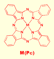 Phthalocyanine Based Molecular Diodes Phthalocyanine Based Molecular Diodes
We have recently created a primative molecular diode based entirely on a class of molecular semiconductors known as metallophthalocyanines, (MPc). Metallophthalocyanines are coordination compounds in which a central transition metal is coordinated to a large, planar macrocyclic tetradentate ligand known as phthalocyanine. In crystalline films of metallophthalocyanines the rings stack on top of one another creating bands of p-orbitals capable of delocalizing ele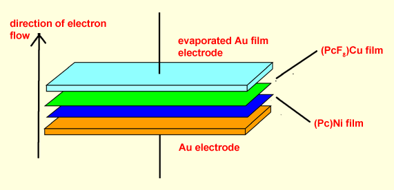 ctron density throughout the entire film. As a result, thin films of metallophthalocyanine are semiconductive. We discovered that junctions between thin films of two differently substituted metallophthalocyanine rings, Cu(PcF8) and Ni(Pc), act as diode junctions, allowing current to pass preferentially in one direction. We are continuing to explore the basic properties of diode junctions formed between a variety of metallophthalocyanine based molecular semiconductors and conventional semiconductor films. ctron density throughout the entire film. As a result, thin films of metallophthalocyanine are semiconductive. We discovered that junctions between thin films of two differently substituted metallophthalocyanine rings, Cu(PcF8) and Ni(Pc), act as diode junctions, allowing current to pass preferentially in one direction. We are continuing to explore the basic properties of diode junctions formed between a variety of metallophthalocyanine based molecular semiconductors and conventional semiconductor films.
Phthalocyanine Based Redox Catalysts and Chemical Sensors
Square planar metallophthalocyanines are capable of coordinating Lewis bases at the axial sites. Thus, semiconducting films of various M(Pc)s can act as redox catalysts on the surface of an elec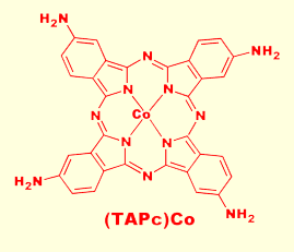 trode. We found that tetraaminophthalocyaninatocobalt(II), (TAPc)Co, shown to the left, acts as an effective electrocatalyst for the reduction of N2O to N2 on the surface of graphite electrodes. The cobalt center coordinates the N2O molecule while the electron rich pi system of the Pc ring facilitates electron transfer. M(Pc) films are particularaly attractive as electrocatalysts because the energy of the pi system is greatly affected by peripheral substituents. The presence of the four amino groups on the ring renders the pi system electron rich, and results in a strong reduction catalyst. Cons trode. We found that tetraaminophthalocyaninatocobalt(II), (TAPc)Co, shown to the left, acts as an effective electrocatalyst for the reduction of N2O to N2 on the surface of graphite electrodes. The cobalt center coordinates the N2O molecule while the electron rich pi system of the Pc ring facilitates electron transfer. M(Pc) films are particularaly attractive as electrocatalysts because the energy of the pi system is greatly affected by peripheral substituents. The presence of the four amino groups on the ring renders the pi system electron rich, and results in a strong reduction catalyst. Cons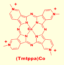 equently, by making the pi system electron deficient, we created a powerful oxidation catalyst. Thus, we found that semiconducting films of the cobalt phthalocyanine derivative, (Tmtppa)Co, shown to the right, catalyse the oxidation of hydrazine and hydroxylamine to N2. As with the (TAPc)Co, (Tmtppa)Co first coordinates the ligand, but in this case holes are transfered from the electrode oxidizing the coordinated amine. One obvious industrial application of this chemistry is in the area of chemical sensing. By monitoring the open cell potential of an M(Pc) modified graphite electrode, one can detect the presence of trace amounts of target compound. We have thus far created M(Pc) based sensors for O2, CO, CO2, NO, N2O, NO2, and S2-, and are currently researching the possibility of creating highly sensitive and highly selective M(Pc) based thiol sensors for detecting the metabolites of bacteria. Such sensors may find application for the detection of mouth and gingiva infections. equently, by making the pi system electron deficient, we created a powerful oxidation catalyst. Thus, we found that semiconducting films of the cobalt phthalocyanine derivative, (Tmtppa)Co, shown to the right, catalyse the oxidation of hydrazine and hydroxylamine to N2. As with the (TAPc)Co, (Tmtppa)Co first coordinates the ligand, but in this case holes are transfered from the electrode oxidizing the coordinated amine. One obvious industrial application of this chemistry is in the area of chemical sensing. By monitoring the open cell potential of an M(Pc) modified graphite electrode, one can detect the presence of trace amounts of target compound. We have thus far created M(Pc) based sensors for O2, CO, CO2, NO, N2O, NO2, and S2-, and are currently researching the possibility of creating highly sensitive and highly selective M(Pc) based thiol sensors for detecting the metabolites of bacteria. Such sensors may find application for the detection of mouth and gingiva infections.
Electroluminscent Polymers
Some materials exhibit the property of electroluminescence, the emission of light when subjected to an applied voltage. Electroluminscence differs from incandescence, which is the black-body radiation emitted from a h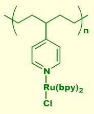 eated object (like in a conventional light bulb), fluorescence, which is the light emitted from some materials when stimulated by a higher energy light source (like in a fluorescent lamp), and cathodoluminescence - emission due to high energy electron bombardment, as in a television or computer screen (unless you have a LCD display, the light you're looking at right now is cathodoluminescence). Electroluminescent panels are commercially available, and offer many advantages over LED, incandescent, fluorescent, or cathodoluminescent light sources. They can be made large or small, they are flat and thin, the light can be rapidly modulated, and they are available in a few different colors. These properties make electroluminescent panels ideal candidates for heads-up displays, front panel displays for electronic equipment (the Timex Indiglo watch uses an electroluminescent panel), and flat-screen TV. Conventional electroluminescent panels are constructed from atomically doped semiconductors such as ZnS:Cu or ZnS:Mn. The electronically excited dopant at eated object (like in a conventional light bulb), fluorescence, which is the light emitted from some materials when stimulated by a higher energy light source (like in a fluorescent lamp), and cathodoluminescence - emission due to high energy electron bombardment, as in a television or computer screen (unless you have a LCD display, the light you're looking at right now is cathodoluminescence). Electroluminescent panels are commercially available, and offer many advantages over LED, incandescent, fluorescent, or cathodoluminescent light sources. They can be made large or small, they are flat and thin, the light can be rapidly modulated, and they are available in a few different colors. These properties make electroluminescent panels ideal candidates for heads-up displays, front panel displays for electronic equipment (the Timex Indiglo watch uses an electroluminescent panel), and flat-screen TV. Conventional electroluminescent panels are constructed from atomically doped semiconductors such as ZnS:Cu or ZnS:Mn. The electronically excited dopant at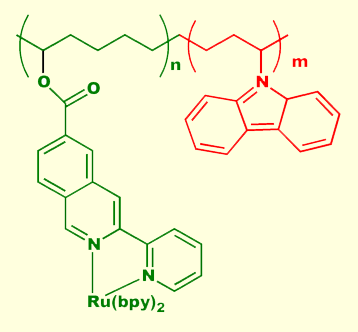 om is the actual light source; the purpose of the semiconductor is to provide a matrix for the electrons to move freely. Excitation of the dopant occurs via electron impact. We have recently discovered that the transition metal moiety bisbipyridinechlororuthenium (III), illustrated above left, coordinated to a semiconductive polymer can be placed directly into an excited state by electron capture from the polymer's conduction band. Relaxation of the excited state occurs with light emission and subsequent hole capture from the polymer's valence band. Light emission continues under the influence of an electric field sourcing electrons to the conduction band and holes to the valence band. Our continuing research in this area is directed towards the synthesis and study of novel transition metal containing electroluminophores coordinated to a variety of different semiconductive polymers. Although scientifically interesting, this material is not useful in a practical device due to low quantum yield. The primary problem is carrier mobility. In an effort to increase hole conductivity to the ruthenium center, we created a series of alternating block copolymers, as shown on the right. The block in green is the emissive center, while the block in red enhances hole mobility through the polymer chain. Our preliminary studies have shown all of our polypyridyl containing polymers to be electroluminescent. We are now in the process of quantifying the electroluminescent behavior of these novel and interesting systems. om is the actual light source; the purpose of the semiconductor is to provide a matrix for the electrons to move freely. Excitation of the dopant occurs via electron impact. We have recently discovered that the transition metal moiety bisbipyridinechlororuthenium (III), illustrated above left, coordinated to a semiconductive polymer can be placed directly into an excited state by electron capture from the polymer's conduction band. Relaxation of the excited state occurs with light emission and subsequent hole capture from the polymer's valence band. Light emission continues under the influence of an electric field sourcing electrons to the conduction band and holes to the valence band. Our continuing research in this area is directed towards the synthesis and study of novel transition metal containing electroluminophores coordinated to a variety of different semiconductive polymers. Although scientifically interesting, this material is not useful in a practical device due to low quantum yield. The primary problem is carrier mobility. In an effort to increase hole conductivity to the ruthenium center, we created a series of alternating block copolymers, as shown on the right. The block in green is the emissive center, while the block in red enhances hole mobility through the polymer chain. Our preliminary studies have shown all of our polypyridyl containing polymers to be electroluminescent. We are now in the process of quantifying the electroluminescent behavior of these novel and interesting systems.
|


 tofore unheard-of electronic devices such as single electron transistors and UV light emitting diodes. Our research in this area has focused on (1) the chemical functionalization of the surface of the nanocluster spheres, and (2) determining the chemical activity of the surface funtionalitites. Thus far, we have successfully created a number of surface functionalized CdS quantum dots, and demonstrated that the functionalities can be used to covalently anchor interesting moieties, such as dyes, electroactive molecules, luminophores, and transition metal complexes, onto the nanocluster surface. We have even demonstrated that surface functionalities can be used to polymerize quantum dots. We have also demonstrated that the surface functionalities are in facile electronic communication with the semiconductor core, and the surface groups are even in direct electronic communication with each other through the core. Our most recent research involves the emissive properties of these interesting systems. We hope that our research in this area may lead to a better understanding of the electronic relationships between the nanocluster core and surface structures, and perhaps lead to the creation of new and unusual electronic devices.
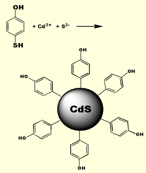 We form our nanoclusters via the so-called kinetic trapping method. Cadmium ion is precipitated with sulfide in the presence of a substituted thiol. During precipitation, a competition occurs between sulfide and thiolate (formed from the sulfide induced deprotonation of the thiol) to condense with the cadmium cation. The thiolate sulfur is softer than sulfide and thus binds to the soft Cd2+ faster. Eventually, the thiolates completely encapsulate the CdS cluster and arrest further growth of the nanocrystal. By adjusting the mole ratio of sulfide to thiolate, one can control the size of the nanocluster. Typical sizes range between 10 and 40 angstroms. Once attached, the surface groups are chemically active and can be used as an anchor to tether a
 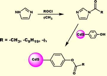 variety of electron withdrawing, electron donating, redox active, or optically interesting moieties. CdS quantum confined nanoclusters are, however, quite sensitive to harsh reaction conditions. Thus, our group has worked out a number of methodologies for carrying out surface reactions under such conditions as to not disrupt the integrety of the nanocluster. One such method involves the reaction of a phenolic surface quantum dot with an N-acylimidazole. With this method a wide variety of groups can be tethered to the surface of the nanocluster. More
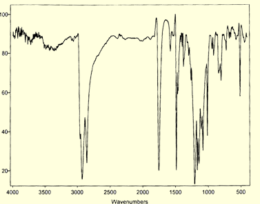 over, small molecule spectroscopy can be used to characterize the surface. For example, the IR spectrum of the decanoyl esterified phenolic quantum dot is shown below. The IR spectrum clearly shows vibrational bands arising from the aromatic and aliphatic sections of the capping groups. Two important features to note in the IR spectrum are the presence of the strong ester carbonyl stretching vibration, and the almost complete absence of a phenolic hydroxyl band, indicating near quantitative esterification of the surface groups. 1H-NMR spectroscopy is particularly informative. Not only are the proton resonances fully assignable, but they appear considerably broadened, due to the hindered tumbling rate of the large nanocluster on the NMR timescale. This is further evidence that the functionalization group is covalently bound to the surface and not in dynamic equilibrium with solution phase species. Below is the 1H-NMR spectrum of an aniline s
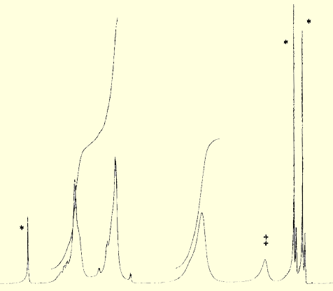 urface CdS nanocluster. Note the homogeneously broadened proton resonances of the surface bound groups as compared to the sharp resonances of the solvent residuals (marked with *).
 polyamide sol-gels (Jello). The sol-gels we work with are crosslinked chains of tetrahedral silicon dioxide. They are easily formed by the slow, controlled hydrolysis of tetraalkoxysilanes. Initially, the hydrolysis results in the formation of linear chains of silicate (the sol). The sol is then kept at slightly elevated temperature for several days, during which time the
  linear chains crosslink to form the gel. The gel is actually a three-dimensional solid matrix encapsulating voids filled with aqueous methanol. At this point the gel has the consistancy of Jello. The gel then enters the drying phase where the aqueous methanol evaporates promoting further crosslinking and causing the gel to physically shrink. At temperatures below about 100 degrees the shrinking process will continue until about 25% of the original volume of aqueous methanol remains in the voids and the gel appears as a transparent solid glassy material. Importantly, any solute dissolved in the aqueous phase will be entrapped in the voids, while any hydrophobic solutes will intercalate in the sol-gel matrix itself. Hence, silicate sol-gels are ideal candidates for the creation of novel electrooptical materials. They are transparent, ionically conductive, and capable of immobilizing hydrophilic and hydrophobic species in separate compartments.